
13. Heap & Stacks sizing
This tutorial is not about FreeRTOS memory management options. All along this tutorials, we've been using the heap_1.c model, that places ourselves into the simplest scheme where neither tasks nor kernel objects are dynamically created and deleted after the scheduler has started. The Heap is dynamically filled when tasks and objects are created during initializations, but never freed later on. This tutorial rather addresses the question of memory sizing at build time for both the Heap and the task Stacks. And there's quite enough to discuss on that topic.
Figure below is an attempt to sketch a "representative" memory layout of an embedded application.
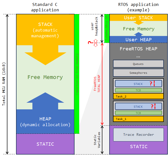
For a standard C application with no RTOS, things are rather simple:
The STATIC segment is used to store everything that is statically allocated at build time. It includes global variables, variables inside functions that have the static attribute, and non-zero initialization values. The exact size of the static segment is therefore known after the build process completes and is summarized into the .data and .bss sections of the build report.
All remaining memory is assumed to be free. Yet, when the program executes:
All the variables local to functions are dynamically created onto the STACK region, that grows and shrinks with the depth of the calling sequence.
All variable that are dynamically created and destroyed by software using malloc() and free() are located on the Heap. Again, the Heap grows and shrinks during execution.
Because both Stack and Heap borders are moving during the program execution, it is common to start each region at both ends of the free memory segment, to get the best chance to maximize the memory usage without collision.
Now, when using an RTOS, things are a little more tricky:
The STATIC region works just the same as above described. And its size is given by the build report.
Then, part of the free memory must be registered for the RTOS operation. In these tutorials, this memory region (FreeRTOS HEAP) is statically allocated, so you can see it as part of the static region. This memory reservoir is empty at build time, just like a standard Heap. That's inside this reservoir that FreeRTOS performs all its dynamic allocations: for system tasks, user tasks (including TCBs and Stacks), kernel objects, ... and everything. Note that variables local to functions (i.e. automatic variables) that are under the RTOS control are stored and managed inside of the task's Stacks. So, no need to say, this FreeRTOS HEAP segment is usually a significant part of the total memory available.
In addition, for everything that operates "outside" the RTOS, we must keep some free space, in which we can dynamically manage a Heap and a Stack the same way as for any standard application. Note that with our project template, you'll get a build error if this remaining free space drops below 1.5kB. This protection is written in the linker script, and if you know what you're doing, you can lower these limits to scrounge some more bytes for your RTOS needs.
/* required amount of heap = 512 bytes  */
_Min_Heap_Size 	= 0x200;
/* required amount of stack = 1024 bytes */
_Min_Stack_Size = 0x400;

...

/* User_heap_stack section, used to check that there is enough RAM left */
._user_heap_stack :
{
    . = ALIGN(8);
    PROVIDE ( end = . );
    PROVIDE ( _end = . );
    . = . + _Min_Heap_Size;
    . = . + _Min_Stack_Size;
    . = ALIGN(8);
} >RAM
This ._user_heap_stack section can be a little misleading because it does not count as free memory region in the build reports, whereas it is actually free.
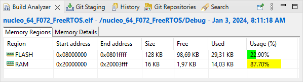
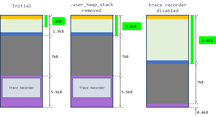
In the above figure, the Heap & Stack memory regions corresponds to the "free memory" according to the build report. Using the demo from the previous tutorial (software timers) for instance, the build reports about 2kB of free space:
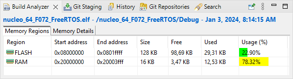
Yet, if we just lower to 0 the .user_heap_stack section in the linker script, nothing changes in the memory layout but we scrounge 1.5kB of additional free space. This reports is more representative of the reality, but we loose the safety net, so you shouldn't do that:
And, just for curiosity, if we disable all the tracing facilities, which are there for debug only, and will likely not be included in a release version of the embedded firmware, we now have more than half of the available memory that is free! Note that if we subtract the 7kB of FreeRTOS Heap that are included in the static section reports, we end up with only 0.41kB (410 bytes) of global variables, mostly for the FreeRTOS internal management.
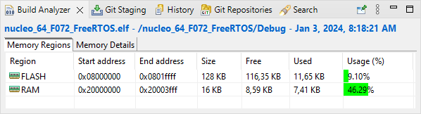
Figure below summarizes the above experiments:
So OK, that story is all marvelous, but why should we care? Well, that's because there are a few things that we must size by ourselves, illustrated by the question marks in the first figure :
The amount memory to register for the FreeRTOS Heap, and consequently, what's left for the user Heap & Stack memory section
Each task Stack
If you have bunch of RAM available, you can easily oversize everything and that will work fine. But in most real-life application, and for obvious money reason, you'll find yourself embedding the MCU that "just" fits your application needs. And then you need a clear strategy for sizing the different memory regions. Where would be the fun otherwise!
1. The Heap
The Heap represents the amount of RAM memory allocated for data placed under FreeRTOS control. It is the one reservoir of bytes that FreeRTOS uses for:
Internal mechanisms and system tasks
User kernel objects data structures (Semaphores, Queues, ...)
User tasks (including TCB and Stacks)
The Heap size is up to you. This is done by defining the configTOTAL_HEAP_SIZE symbol in FreeRTOSConfig.h. At his moment, we have 7kB for the FreeRTOS Heap:
#define configTOTAL_HEAP_SIZE ( ( size_t ) ( 7 * 1024 ) )
How do we size the Heap? There are two possible approaches :
From the "outside": We size the Heap as big as we can once we know (i) how much static variables we have, and (ii) what minimum limit we put on the user Heap & Stack section. That's the simple way to do it, and most of the time the starting point.
From the "inside": We try to evaluate our needs. By sizing the Heap for "what is needed", including a safety margin, we can hopefully provide more free RAM for the user Heap & Stack and then get away from potential crash there. The problem here is that "what is needed" includes task Stacks... and those are somehow difficult to foresee. We usually end-up in an iterative process where we start with an oversized Heap first, then evaluate the task Stacks needs empirically by observing Stacks usage during execution, and then come back adjusting the FreeRTOS Heap to something reasonably safe.
The whole purpose is a fair share of the cake (the memory) among guests (task Stacks, FreeRTOS, user Heap & Stack), so that no one is taking a bigger slide than he can eat, while other are starving. You get the picture? Ideally everybody has just a little more than he can eats... to be at ease.
1.1. Sizing the Heap "from the outside"
The more Heap you have for FreeRTOS, the more room you have to create tasks and kernel objects. So a first move would be to set the heap as big as the amount of RAM permits. In practice, after the static region has been filled, the remaining amount of memory has to be split into (i) the FreeRTOS heap, and (ii) the user Heap & Stack that is required for operation outside the FreeRTOS control. The latter depends on what you do, essentially before starting the scheduler. If main() has few local variables and doesn't call memory demanding functions, then a small user Heap & Stack segment will probably do. A good start then can be the lower limit sets in the linker script. An easy way to get close to the maximum heap you can have is to increase the FreeRTOS heap until you get a linker error (assuming you've kept untouched our safety net in the linker script).
So coming back to our initial situation with the previous tutorial project (.user_heap_stack restored and trace facility enabled), let-us try to increase the FreeRTOS heap. We had a little less than 2kB of free space, to pushing the heap of 8kB we probably pass the build examination:
But trying 9kB won't work:
Lowering the safety net in the linker script would allow the pass the build with 9kB of FreeRTOS heap (we're very close actually, only 32 bytes are missing), but we have to put a limit anyway. Again, we absolutely need a memory section for the user Heap & Stack. If we remove the safety net and get close to 100% of memory usage, the program will probably crash during execution. We absolutely need generous enough free space!
1.2. Sizing the Heap "from the inside"
In the above example (and so far in these tutorials), the heap is set to 7kB (exactly 7168 bytes). Eventually, we've just seen that it could be raised to 8kB.
Is it enough? Is it too much?
Well, I don't know... I just can say "It has to be enough", given that it is close to a maximum considering the static memory needs (especially for trace recording) and the user Heap & Stack section we need to preserve for non-FreeRTOS stuff.
Of course, this is not an acceptable answer. The less heap you have, the more limitations you will face in terms of (i) number of possible kernel objects, (ii) number of possible tasks and (iii) amount of data the tasks can process.
The xPortGetFreeHeapSize() API function returns the amount of free heap bytes. Let-us experiment this using the case study below.
/*
 * main.c
 *
 *  Created on: 01/04/2018
 *      Author: Laurent
 */

#include "main.h"

// Static functions
static void SystemClock_Config	(void);

// FreeRTOS tasks
void vTask1 	(void *pvParameters);
void vTask2 	(void *pvParameters);
void vTaskHWM 	(void *pvParameters);

xTaskHandle	vTask1_handle;
xTaskHandle	vTask2_handle;
xTaskHandle 	vTaskHWM_handle;

// Kernel objects
xSemaphoreHandle xSem;
xSemaphoreHandle xConsoleMutex;
xQueueHandle	 xConsoleQueue;

// Define the message_t type as an array of 64 char
typedef uint8_t message_t[64];

// Trace User Events Channels
traceString ue1, ue2, ue3;

// Main function
int main()
{
	uint32_t	free_heap_size;

	// Configure System Clock
	SystemClock_Config();

	// Initialize LED pin
	BSP_LED_Init();

	// Initialize Debug Console
	BSP_Console_Init();

	// Start Trace Recording
	vTraceEnable(TRC_START);

	// Report Free Heap Size
	free_heap_size = xPortGetFreeHeapSize();
	my_printf("\r\nFree Heap Size is %d bytes\r\n", free_heap_size);

	// Create Semaphore object (this is not a 'give')
	my_printf("\r\nNow creating Binary Semaphore...\r\n");
	xSem = xSemaphoreCreateBinary();
	vTraceSetSemaphoreName(xSem, "xSEM");
	free_heap_size = xPortGetFreeHeapSize();
	my_printf("Free Heap Size is %d bytes\r\n", free_heap_size);

	// Create Queue to hold console messages
	my_printf("\r\nNow creating Message Queue...\r\n");
	xConsoleQueue = xQueueCreate(4, sizeof(message_t));
	vTraceSetQueueName(xConsoleQueue, "Console Queue");
	free_heap_size = xPortGetFreeHeapSize();
	my_printf("Free Heap Size is %d bytes\r\n", free_heap_size);

	// Create a Mutex for accessing the console
	my_printf("\r\nNow creating Mutex...\r\n");
	xConsoleMutex = xSemaphoreCreateMutex();
	vTraceSetMutexName(xConsoleMutex, "Console Mutex");
	free_heap_size = xPortGetFreeHeapSize();
	my_printf("Free Heap Size is %d bytes\r\n", free_heap_size);

	// Register the Trace User Event Channels
	my_printf("\r\nNow registering Trace events...\r\n");
	ue1 = xTraceRegisterString("ticks");
	ue2 = xTraceRegisterString("msg");
	ue3 = xTraceRegisterString("HWM");
	free_heap_size = xPortGetFreeHeapSize();
	my_printf("Free Heap Size is %d bytes\r\n", free_heap_size);

	// Create Tasks
	my_printf("\r\nNow creating Tasks...\r\n");
	xTaskCreate(vTask1,	"Task_1",	128, NULL, 2, &vTask1_handle);
	xTaskCreate(vTask2,	"Task_2",	128, NULL, 3, &vTask2_handle);
	xTaskCreate(vTaskHWM,	"Task_HWM",	128, NULL, 1, &vTaskHWM_handle);
	free_heap_size = xPortGetFreeHeapSize();
	my_printf("Free Heap Size is %d bytes\r\n", free_heap_size);

	// Start the Scheduler
	my_printf("\r\nNow Starting Scheduler...\r\n");
	vTaskStartScheduler();

	while(1)
	{
		// The program should never be here...
	}
}
Then provide an ultra-minimal implementation for the three tasks:
/*
 *	Task_1
 */
void vTask1 (void *pvParameters)
{
	while(1)
	{
		// Wait for 100ms
		vTaskDelay(100);
	}
}

/*
 *	Task_2
 */
void vTask2 (void *pvParameters)
{
	while(1)
	{
		// Wait for 100ms
		vTaskDelay(100);
	}
}

/*
 * vTaskHWM
 */
void vTaskHWM (void *pvParameters)
{
	uint32_t	free_heap_size;

	while(1)
	{
		// Periodically Report Free Heap size after scheduler has started
		free_heap_size = xPortGetFreeHeapSize();
		my_printf("Free Heap Size is %d bytes\r", free_heap_size);

		// Wait for 500ms
		vTaskDelay(500);
	}
}
Now take a look at the console during initializations:
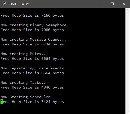
At the beginning of code execution, we've got 7160 bytes available. That's our 7kB of total heap, minus 2 words (we will assume FreeRTOS has good use for these).
Creating the Binary Semaphore takes 80 bytes of heap memory, we've seen that before.
Creating the Message Queue took 336 bytes of heap memory. That's 80 bytes for the object itself, plus 256 bytes for the Queue buffer (4 messages of 64 bytes). You remember why it can be interesting to use pointers instead of full messages?
Creating the Mutex took 80 bytes of heap memory.
Registering trace events took nothing in the heap. Actually, you can have a look in the Memory Details of the build reports and you'll see that trace recording variables are statically allocated is the .bss section.
Creating the three tasks took 1824 bytes of heap memory. That's presumably 608 bytes for each of the 3 tasks. Given that TCB size is 92 bytes and Stacks are 128 words = 512 bytes, the total is 604. We'll live with a 4-bytes delta.
Finally, after the scheduler started, that's 4840-3424 = 1416 extra bytes that are used from the Heap. Actually, FreeRTOS creates internal tasks (such as the IDLE task, timer task, ...) and objects for its internal needs.
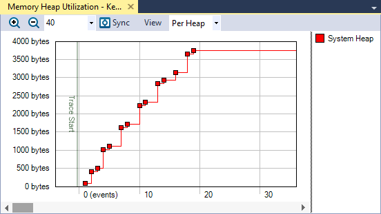
In summary, we need "from the inside" about (7160-3424)/1024 = 3.64kB of Heap memory. So sizing the Heap to 4kB would probably work in this example.
Note that Tracealyzer is able to report the Heap usage, but it is not automatic. You need to place strategic calls to the xPortGetFreeHeapSize() function to get that working:
Let summarize what we have so far:
- Considering (i) the total memory available (16kB), (ii) our needs for static variables (5.5kB) and (iii) the safety net of 1.5kB for the user Heap & Stack section, we can afford a little less than 9kB for FreeRTOS Heap memory. That's the result of the "from the outside" approach.
- By analyzing the real Heap consumption, we've seen that 4kB of FreeRTOS Heap should be enough. That's the result of the "from the inside" approach.
Very well... but there's a big "something" that is missing in this summary...
What about the task Stack? Here we've sized the 3 task Stacks to an arbitrary 128-words = 512 bytes. Is it enough? Is it too much?
Well again, I don't know...
In fact, I know that it is way enough in the above example because our 3 tasks are doing nothing. But in a more general case, it depends on what tasks are actually doing. More precisely, it depends on the amount of data each task is manipulating (either directly using local variables, or indirectly by calling functions that manipulate variables), and what needs to be saved when (or if) task is preempted. Remember that when a task is preempted by another task, the OS saves all the information required for further recovery into the stack.
In the above code, the 3 tasks are pretty much doing nothing. There's no local variables, and a single call to vTaskDelay(). Therefore, a small stack should be enough. But if we need to increase Stacks size, then we also need to increase Heap size, since a Stack is dynamically allocated into the Heap when the task is created.
Time to move on with Stack analysis...
 | - - |
2. Stack High Water Mark
Stacks are used to store task local variables, and any temporary data required for recovery before a task is preempted. Therefore, the amount of instantaneous stack in use continuously fluctuates during application life. FreeRTOS provides a mechanism to calculate the maximum amount of stack memory that has been (at least once) required since the application started.
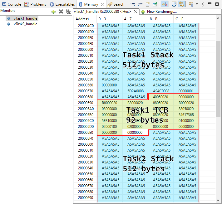
Internally, what this mechanism does is an initial "painting" (at creation time) of the stack RAM segment with a regular pattern. Figure below shows this painting with a uniform 0xA5 pattern (1010 0101). We've seen that before, you remember?
By the way, having this memory layout in plain view, can you figure out what would happen in case of Task2 Stack overflow? Well, that's pretty obvious isn't it? It would flood the Task1 TCB and crash the whole OS... So we have to make sure it won't happen.
When the stack is used (at runtime), the initial painting is overridden (scratched) by meaningful data. The FreeRTOS uxTaskGetStackHighWaterMark() function implements an little algorithm that searches for remaining initial paint within the Stack and then determines the amount of unused Stack. Think of it as a flood in your house. The watermark you get on the walls at a given time corresponds to the highest level the water ever reached. That explains the name for "High Water Mark". The uxTaskGetStackHighWaterMark() function actually return the number of words (4-bytes unit) above the watermark (i.e. the remaining space into the stack).
In order have the uxTaskGetStackHighWaterMark() function available, you first need to activate the mechanism in FreeRTOSConfig.h:
/* Optional functions - most linkers will remove unused functions anyway. */
#define INCLUDE_vTaskPrioritySet                	0
#define INCLUDE_uxTaskPriorityGet               	0
#define INCLUDE_vTaskDelete                     	0
#define INCLUDE_vTaskSuspend                    	0
#define INCLUDE_xResumeFromISR                  	0
#define INCLUDE_vTaskDelayUntil                 	1
#define INCLUDE_vTaskDelay                      	1
#define INCLUDE_xTaskGetSchedulerState          	0
#define INCLUDE_xTaskGetCurrentTaskHandle       	1
#define INCLUDE_uxTaskGetStackHighWaterMark     	1	// <- Check this definition
#define INCLUDE_uxTaskGetStackHighWaterMark2    	0
#define INCLUDE_xTaskGetIdleTaskHandle          	0
#define INCLUDE_eTaskGetState                   	0
#define INCLUDE_xEventGroupSetBitFromISR        	1
#define INCLUDE_xTimerPendFunctionCall          	0
#define INCLUDE_xTaskAbortDelay                 	0
#define INCLUDE_xTaskGetHandle                  	0
#define INCLUDE_xTaskResumeFromISR              	0
If you wonder, note that the uxTaskGetStackHighWaterMark2() function only release restrictions with 8-bit architectures and is of no interest for us now.
Let-us now experiment this. The purpose of the Task_HWM is actually to periodically report the high watermarks for both Task_1, Task_2 and itself into the console.
/*
 * vTaskHWM
 */
void vTaskHWM (void *pvParameters)
{
	uint32_t	count;
	uint16_t	hwm_Task1, hwm_Task2, hwm_TaskHWM;
	uint32_t	free_heap_size;

	count = 0;

	// Prepare console layout using ANSI escape sequences
	my_printf("%c[0m",   0x1B);	// Remove all text attributes
	my_printf("%c[2J",   0x1B); 	// Clear console
	my_printf("%c[1;0H", 0x1B);	// Move cursor [1:0]

	my_printf("High Water Marks console");

	my_printf("%c[3;0H", 0x1B);	// Move cursor line 3
	my_printf("Iteration");

	my_printf("%c[4;0H", 0x1B);	// Move cursor line 4
	my_printf("Task1");

	my_printf("%c[5;0H", 0x1B);	// Move cursor line 5
	my_printf("Task2");

	my_printf("%c[6;0H", 0x1B);	// Move cursor line 6
	my_printf("TaskHWM");

	my_printf("%c[7;0H", 0x1B);	// Move cursor line 7
	my_printf("Free Heap");


	while(1)
	{
	  // Gather High Water Marks
	  hwm_Task1	= uxTaskGetStackHighWaterMark(vTask1_handle);
	  hwm_Task2 	= uxTaskGetStackHighWaterMark(vTask2_handle);
	  hwm_TaskHWM	= uxTaskGetStackHighWaterMark(vTaskHWM_handle);

	  // Get free Heap size
	  free_heap_size = xPortGetFreeHeapSize();

	  // Reports watermarks into Trace Recorder
	  vTracePrintF(ue3, (char *)"1[%d] 2[%d] HWM[%d]",
                             hwm_Task1,
                             hwm_Task2,
                             hwm_TaskHWM );

	  // Display results into console
	  my_printf("%c[0;31;40m", 0x1B); 	// Red over black

	  my_printf("%c[3;12H", 0x1B);
	  my_printf("%5d", count);

	  my_printf("%c[1;33;44m", 0x1B); 	// Yellow over blue

	  my_printf("%c[4;12H", 0x1B);
	  my_printf("%5d", hwm_Task1);

	  my_printf("%c[5;12H", 0x1B);
	  my_printf("%5d", hwm_Task2);

	  my_printf("%c[6;12H", 0x1B);
	  my_printf("%5d", hwm_TaskHWM);

	  my_printf("%c[1;35;40m", 0x1B); 	// Majenta over black
	  my_printf("%c[7;12H", 0x1B);
	  my_printf("%5d", free_heap_size);

	  my_printf("%c[0m", 0x1B); 		// Remove all text attributes
	  count++;

	  // Wait for 200ms
	  vTaskDelay(200);
	}
}
I couldn't resist playing with ANSI escape sequences to bring some fun into the console display, although this not quite essential here.
Still, if you like it, see more there: https://en.wikipedia.org/wiki/ANSI_escape_code
The console then reports:
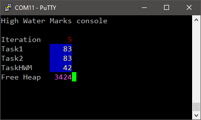
The remaining amount of Stack for each task (in 4-bytes words)
The remaining amount of Heap (in bytes)

None of the above is zero, or even close to zero, therefore, I can now temporarily answer the questions:
Do we have Heap memory enough? → Yes, maybe too much actually.
Do we have Stack memory enough? → Yes, but not too much as we should stay somehow far from zero. Both Stacks associated with Task_1 and Task_2 have been used for up to 45 words (128-83). Also note that 128 words is the minimal stack size defined by default in FreeRTOSConfig.h. We can now understand why since a task basically doing nothing still "consumes" about half of this minimum.
#define configMINIMAL_STACK_SIZE ( ( uint16_t ) 128 )
Of course, the above answers are only valid for the current application, which does actually nothing useful. If we want the tasks to perform something real, answers would be different. I think you get the point.
Now, let us shorten Task_1 and Task_2 wake-up period in order to increase the density of Task_HWM preemption events:
/*
 *	Task_1
 */
void vTask1 (void *pvParameters)
{
	while(1)
	{
		// Wait for 20ms
		vTaskDelay(20);
	}
}

/*
 *	Task_2
 */
void vTask2 (void *pvParameters)
{
	while(1)
	{
		// Wait for 30ms
		vTaskDelay(30);
	}
}
Launch the application and watch the console. Reaching iteration #4, the watermark for Task_HWM drops from 49 to 42. Something we didn't observe previously even leaving the application running for more than 100 iterations...
As said before, the Stack is used to save task information when it is preempted. Therefore, the amount of data to save totally depends on the very moment the preemption occurs. Considering Task_HWM, there is a strong probability that preemption occurs during a call to my_printf() function. In that case, the current state (variables) of my_printf() function are saved into Task_HWM stack. If you're not lucky, you might never catch the worst situation.
What the above experiment demonstrates, is:
You will never be 100% sure that watermarks you get represents the worst case of Stack usage
The longer you'll leave application running, trying to cover a lot of application situations, the closer you should get from the 'true' worst case
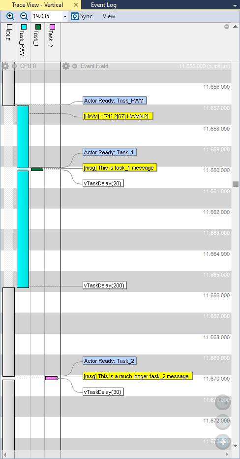
Now, let us add some data into Task_1 and Task_2:
/*
 *	Task_1
 */
void vTask1 (void *pvParameters)
{
	uint8_t	msg[] = "This is task_1 message"; // 22 bytes string

	while(1)
	{
		// Send message to Trace Recorder
		vTracePrint(ue2, (char *)msg);

		// Wait for 20ms
		vTaskDelay(20);
	}
}

/*
 *	Task_2
 */
void vTask2 (void *pvParameters)
{
	uint8_t	msg[] = "This is a much longer task_2 message"; // 36 bytes string

	while(1)
	{
		// Send message to trace Recorder
		vTracePrint(ue2, (char *)msg);

		// Wait for 30ms
		vTaskDelay(30);
	}
}
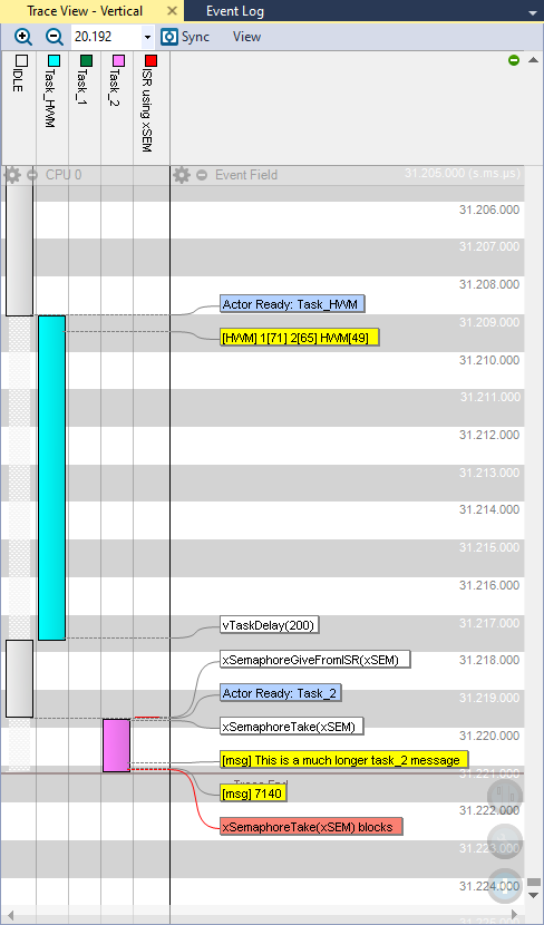
The corresponding trace:
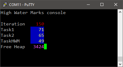
And our HWM console after 60 iterations:

High watermarks dropped from the previous 83 for both Task_1 and Task_2 tasks to 71 and 67 respectively. The stored strings for Task_1 is 22+1 bytes long, so that's 6 additional words taken into its Stack. For Task_2, that's (36+1)/4 = 10 additional words. That explains the 4 words difference we now have between Task_1 and Task_2.
Yet (82-6) = 76 and (82-10) = 72 so that an additional load of 5 words (20 bytes) haven been used in both Stacks. One can guess that calling vTracePrint() function has its own footprint into the Stack.
| - - |
3. Crash Tests
3.1. Insufficient Heap
According the above measurements, we need 7168-3424 = 3744 bytes of heap memory to fit all the kernel objects and tasks in our application.
What if we set the heap size below this requirement?
Well, let us experiment with 3.5kB of heap memory:
#define configTOTAL_HEAP_SIZE ( ( size_t ) ( 3584 ) )
Build ![]() the application. You should no get any error or warning. Then start a debug session
the application. You should no get any error or warning. Then start a debug session ![]() and step over
and step over ![]() initialization code. Everything goes well until you start the scheduler. Then, the application freezes. Hit the suspend
initialization code. Everything goes well until you start the scheduler. Then, the application freezes. Hit the suspend ![]() button:
button:
Well, at least, that's pretty clear... Depending on how much Heap is missing, you might as well end up in another failing assertion (while creating the internal timer task for instance, with less explicit comments).
On a side note, you should know that you can implement your own function the handle failed assertions and get reporting directly into the console. Just paste this function at the end of main.c:
/*
 * Assertion Handler
 */
void vAssertCalled( char *file, int line )
{
	taskDISABLE_INTERRUPTS();

	my_printf("Assertion Failed\r\n");
	my_printf("File %s\r\n", file);
	my_printf("Line %d\r\n", line);

	while(1);
}
Then in FreeRTOSConfig.h, locate the macro that currently defines the configASSERT(x) function and replace it with a call to our vAssertCalled() function:
/* Define to trap errors during development. */
void vAssertCalled(char *file, int  line);
// #define configASSERT(x) if( ( x ) == 0 ) { taskDISABLE_INTERRUPTS(); for( ;; ); }
#define configASSERT(x) if( ( x ) == 0 ) vAssertCalled( __FILE__, __LINE__ )
Build ![]() the application and run it
the application and run it ![]() directly:
directly:
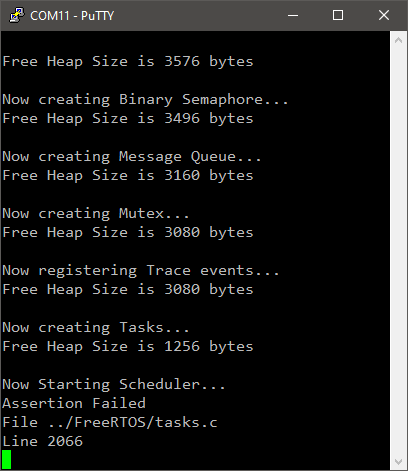
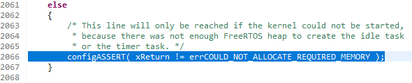
Well done! You can double-check, that's the correct line in task.c.
Coming back to our subject, consider you're lucky if the scheduler didn't start. Way more dangerous is the case everything starts well, but you fail creating a kernel objects during application life (i.e. after scheduler is started). As a matter of fact, nothing impose kernel objects to be created at initialization.
One way to address such issue would be to implement a dynamic memory allocation failure hook function. First, you must enable this feature in FreeRTOSConfig.h by enabling configUSE_MALLOC_FAILED_HOOK:
/* Hook function related definitions. */
#define configUSE_IDLE_HOOK                     	0
#define configUSE_TICK_HOOK                     	0
#define configCHECK_FOR_STACK_OVERFLOW          	0
#define configUSE_MALLOC_FAILED_HOOK            	1	// <- Check this definition
#define configUSE_DAEMON_TASK_STARTUP_HOOK      	0
#define configUSE_SB_COMPLETED_CALLBACK         	0
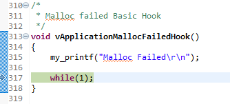
Then, you'll need to provide your own implementation of the function vApplicationMallocFailedHook(). Let us write something basic in main.c: This hook does nothing, but at least it provides a way to catch the problem in the debugger.
/*
 * Malloc failed Basic Hook
 */
void vApplicationMallocFailedHook()
{
	my_printf("Malloc Failed\r\n");

	while(1);
}
Repeat the above experiment now. After the program freezes, hit the suspend ![]() button. I you should end-up in your hook function:
button. I you should end-up in your hook function:
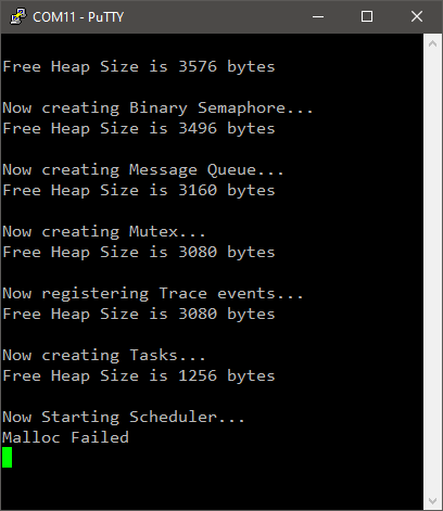
In a real scenario, you can use such hook to allow the watchdog to reset the application and use that information to avoid further attempts to create the failing object.
| - - |
For now, just restore Heap size to 7kB before proceeding to next experiment.
3.2. Stack overflow
Say now we need to call a function that requires its own amount of memory to execute. For instance, let us computes the cumulative weighted sum of an array of integers. Put the following function at the end of main.c and add its prototype at the beginning:
/*
 * sum_prod function
 *
 * Calculate y the sum of (x * coef[n])
 * x is a floating point number
 * coef[n] is an array of 120 32-bit integers
 *
 * returns y a floating point number
 */
float sum_prod(float x)
{
	uint32_t 	coef[120];
	float		y;
	uint8_t		n;

	// Initialize array
	for (n=0; n<120; n++) coef[n] = n;

	// Calculate sum of products
	y = 0;
	for (n=0; n<120; n++) y += x * coef[n];

	return y;
}
Now, we implement a call to this function within Task_2, but only if the user push-button is pressed. To do that, we'll use the EXTI #13 interrupt signal to give a semaphore to Task_2:
/*
 *	Task_2
 */
void vTask2 (void *pvParameters)
{
	uint8_t		msg[] = "This is a much longer task_2 message"; // 36 bytes string
	float 		x,y;

	// Initialize the user Push-Button
	BSP_PB_Init();

	// Set maximum priority for EXTI line 4 to 15 interrupts
	NVIC_SetPriority(EXTI4_15_IRQn, configMAX_API_CALL_INTERRUPT_PRIORITY + 1);

	// Enable EXTI line 4 to 15 (user button on line 13) interrupts
	NVIC_EnableIRQ(EXTI4_15_IRQn);

	// Take the semaphore once to make sure it is cleared
	xSemaphoreTake(xSem, 0);

	// Now enter the task loop
	while(1)
	{
		// Wait here endlessly until button is pressed
		xSemaphoreTake(xSem, portMAX_DELAY);

		// Compute y
		x = 1.0f;
		y = sum_prod(x);

		// Send message to trace Recorder
		vTracePrint (ue2, (char *)msg);
		vTracePrintF(ue2, (char *)"%d", (uint32_t)y);
	}
}
Make sure that EXTI #13 interrupt handler is well written in stm32f0xx_it.c:
/**
  * This function handles EXTI line 13 interrupt request.
  */

extern xSemaphoreHandle xSem;

void EXTI4_15_IRQHandler()
{
	portBASE_TYPE xHigherPriorityTaskWoken = pdFALSE;

	// Test for line 13 pending interrupt
	if ((EXTI->PR & EXTI_PR_PR13_Msk) != 0)
	{
		// Clear pending bit 13 by writing a '1'
		EXTI->PR = EXTI_PR_PR13;

		// Release the semaphore
		xSemaphoreGiveFromISR(xSem, &xHigherPriorityTaskWoken);

	    // Perform a context switch to the waiting task
	    portEND_SWITCHING_ISR(xHigherPriorityTaskWoken);
	}
}
And leave Task_1 as something minimal:
/*
 *	Task_1
 */
void vTask1 (void *pvParameters)
{
	uint8_t	msg[] = "This is task_1 message"; 	// 22 bytes string

	while(1)
	{
		// Send message to Trace Recorder
		vTracePrint(ue2, (char *)msg);

		// Wait for 100ms
		vTaskDelay(100);
	}
}
Build and fire the application. Watch the console reporting watermarks (do not press the button yet). You should see your watermarks at safe level, and everything doing good as expected.

Now press the user-button... and something bad should happen!
Depending on 'when' the button is pressed, you may experience two different behaviors.
Case #1 : Application crash
In that case, the console just freezes after you pressed the button:
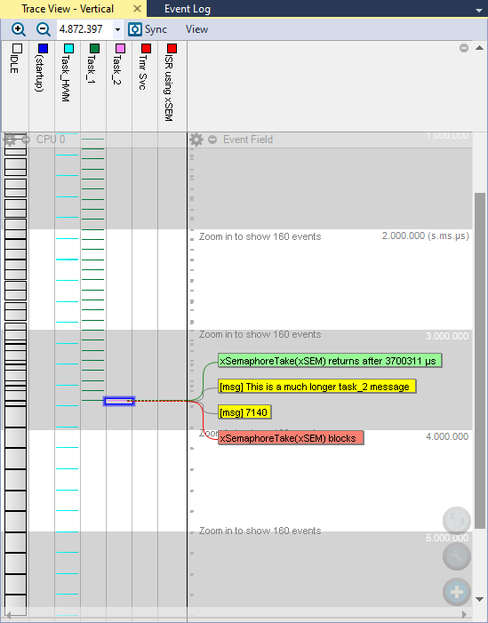
Looking at the trace, you'll see that Task_2 execution was the very last event to be recorded, and then nothing... Application has died, silently...
If you're curious enough to suspend the debugger there, you may find out what the application is doing. Results differ depending on the very moment you pressed the button.
Case #2 : Application keeps running but watermarks dropped to zero
In that case, the Task_HWM keeps running and reports both stacks remaining space to zero:

Which is confirmed by the trace. After the button was pressed, Task_1 crashed and only Task_HWM keeps running.
The reason Task_2 Stack overflew is quite obvious. Calling the sum_prod() function requires the Stack size to cope with a large array of 120 32-bit integers which by itself would almost completely fill the Stack. Then, as it was anticipated considering the memory layout, the overfow of Task_2 Stack probably flood both Task_1 TCB and own Stack creating a complete mess in all the Task_1 data structure. Since Task_HWM is "on the other side of the flood" in memory, it might has been preserved...
This is bad anyway. But again, what the above experience teaches, is that we can easily miss Stack overflow. What if we didn't test button case? All would have looked very fine.
FreeRTOS can help you track stack overflows. First go to FreeRTOSConfig.h and enable configCHECK_FOR_STACK_OVERFLOW the feature:
#define configCHECK_FOR_STACK_OVERFLOW 1
Then, you'll need to provide your own implementation of the function vApplicationStackOverflowHook(). Let us write something basic in main.c:
/*
 * Stack Overflow Basic Hook
 */
void vApplicationStackOverflowHook(TaskHandle_t xTask, char *pcTaskName)
{
    my_printf("Task Overflow in %s\r\n", pcTaskName);
    while(1);
}
Unfortunately, depending on the severity of the problem, the hook does not always work. You may end up into the Hardfault handler as well...
| - - |
4. Summary
When your application crashes, which always happens, sooner or later, during its development, it is not always easy to sort out the cause when working with an RTOS. Failing dynamic allocations and Stack overflows can produce very unexpected and odd behavior. When you're lucky you can catch the problem within a hook or an assertion handler, but most usually the program just goes crazy with odd behavior, or fall into the Hardfault handler with no clue for what reason, or even worse... seems to work and it's only a matter of time before the bad things occur.
Very often, the root cause is a bad memory sizing. Through the course of this tutorial, we've seen how to approach that question of both Heap and Stack sizing with caution and awareness. Monitoring the Stacks watermarks during execution is almost mandatory while writing and testing new code. Without doing so, we're blind. Here, we've done that with the console but you can also get the real time Stack usage within the recorder trace.
That, and trace streaming are addressed in the next (and last) tutorial of this series.